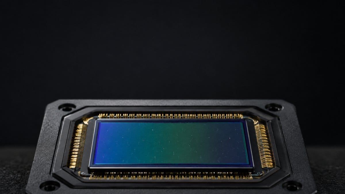
Quick answer: A back illuminated sensor (BSI) is a CMOS chip flipped during manufacturing so light strikes the photodiodes directly, instead of passing through the wiring layer first. That one change lifts quantum efficiency from roughly 50% to 80–90%+, which is why virtually every modern astronomy camera uses a BSI sensor.
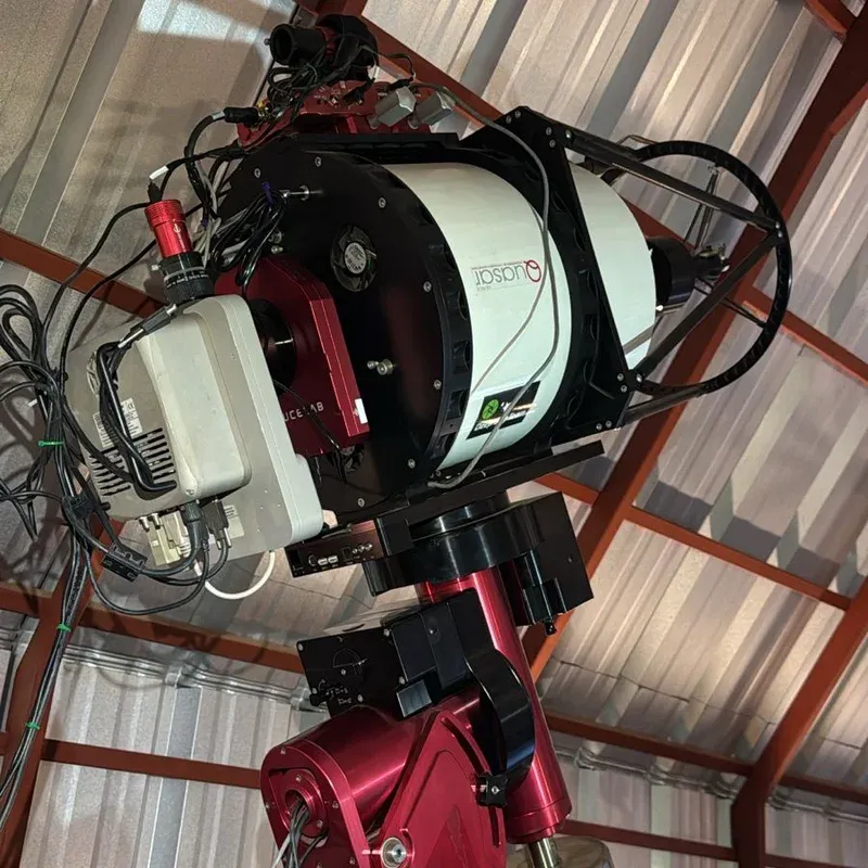
Every photon you collect under a dark sky fought its way across space for years — sometimes millions of years. The last two microns of that journey, through the surface of your camera's sensor, decide whether it becomes signal or waste heat. In this guide we unpack what a back illuminated sensor actually is, how it differs from the front-illuminated (FSI) designs it replaced, and why the BSI revolution quietly transformed amateur astrophotography over the past decade. We run BSI sensors every clear night on our remote rig at DeepSky Chile, so we will also get specific about the chips you are most likely to buy.
This post sits in the accessible tier: no electronics background needed, and we define every term as we go. If you already know your way around quantum efficiency curves, the astrophotography-specific sections in the second half are where the practical payoff lives.
What Is a Back Illuminated Sensor?
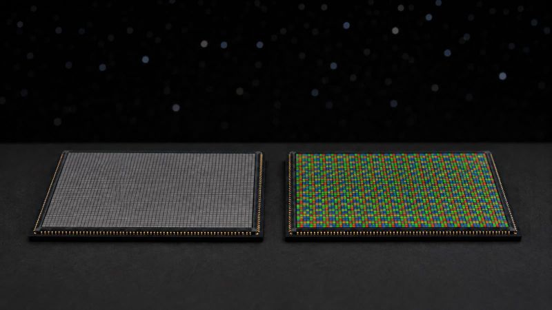
A back illuminated sensor (also written backside illuminated, BSI, or BI) is a CMOS image sensor manufactured so that incoming light reaches the light-sensitive photodiodes from the back of the silicon wafer — the side with no metal wiring in the way. The one-sentence version of BSI vs FSI: in a front-illuminated sensor light must squeeze past the wiring to reach the photodiode, while in a back-illuminated sensor the chip is flipped so light lands on the photodiode first.
"BSI" on a spec sheet simply stands for Backside Illumination. It says nothing about pixel size, resolution, or noise by itself — it describes where the light enters the pixel relative to the electronics.
That sounds like an obscure fabrication detail. It is not. It is the single biggest reason a modern dedicated astronomy camera detects 80–90% of the photons that hit it, while the CCD and early CMOS cameras many of us started with captured barely half.
How a CMOS Pixel Actually Collects Light
To see why flipping the chip matters, you need a picture of what one pixel looks like in cross-section. A CMOS pixel is a layered sandwich, and the order of the layers is the whole story.
Photodiode, wiring layer, and microlenses
Each pixel contains three functional layers:
- The photodiode — a region of silicon that converts photons into electrons. This is the part doing the actual astronomy.
- The wiring layer — several levels of metal interconnects and transistors that read the accumulated charge out of the pixel. CMOS sensors put amplifier circuitry at every pixel, which is what makes them fast and low-noise, but all that circuitry has to live somewhere.
- The microlens — a tiny lens on top of each pixel that funnels incoming light toward the sensitive area, with a color filter beneath it on one-shot-color sensors.
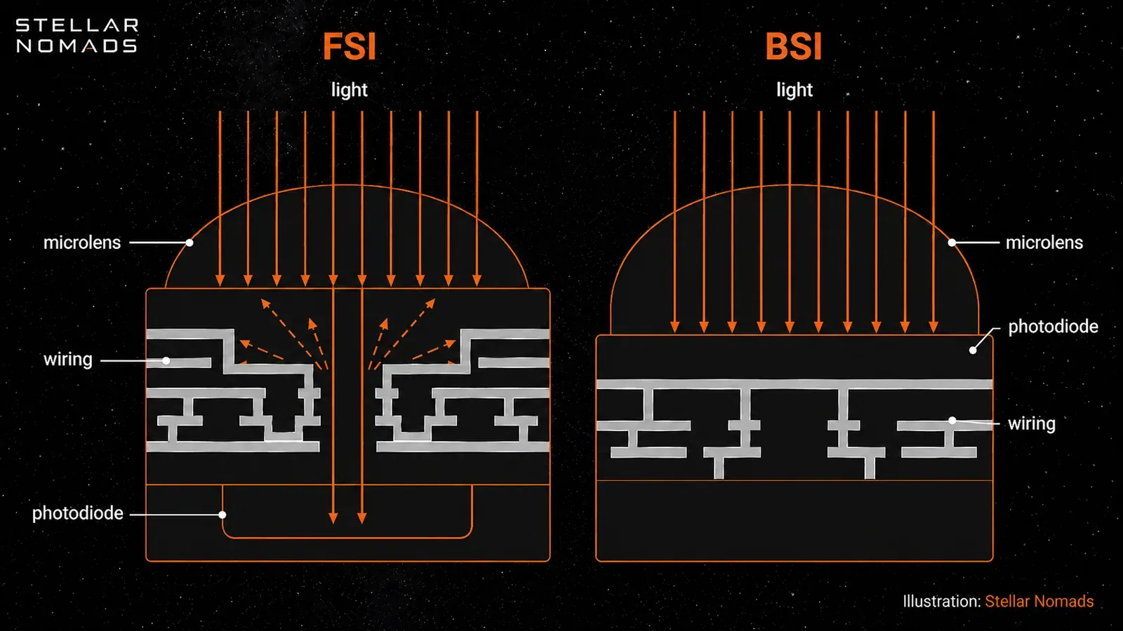
In a conventional front-illuminated design, the manufacturing process naturally leaves the wiring on top, because that is the side of the wafer the circuitry was built on. Light must therefore travel down through a canyon of metal before reaching the photodiode at the bottom.
Where photons get lost in an FSI pixel
Picture a photon arriving at a front side illuminated sensor. Three bad things can happen before it ever reaches silicon:
- Reflection — it bounces off a metal trace and is simply lost.
- Absorption — it is soaked up by the dielectric layers between the wiring, contributing nothing.
- Scatter into a neighbor — it ricochets into the adjacent pixel, registering as faint signal in the wrong place.
The fraction of a pixel's surface genuinely open to light is called the fill factor, and in FSI designs it can drop below 50% for small pixels. Combined with reflection and absorption losses, a typical front-illuminated sensor converts only 40–60% of incoming photons into signal. For daytime photography, wasting half the light is an inconvenience you fix with a longer exposure. For someone imaging a magnitude-14 galaxy, it is half the night thrown away.
FSI vs BSI: The Flip That Changed Everything
The fix sounds almost comically simple: turn the chip over. If the wiring blocks light from the front, illuminate the sensor from the back, where there is nothing but silicon between the sky and the photodiode.
The manufacturing trick: thinning the wafer
The reason nobody did this for decades is that the "back" of a finished wafer is hundreds of microns of bulk silicon — far too thick for light to penetrate to the photodiodes. Making BSI work means bonding the finished wafer face-down to a carrier, then grinding and chemically etching the back down to a few microns, stopping with near-atomic precision just above the photodiode layer. Get it wrong by a hair and you destroy every sensor on the wafer.
Scientific labs did exactly this by hand for observatory CCDs — at heroic cost. The breakthrough was industrializing it. Sony shipped the first mass-produced back-illuminated CMOS sensor, the Exmor R, in 2009, and smartphones adopted BSI almost immediately because their tiny pixels suffered worst from wiring obstruction. Sensor manufacturing itself has deep space-program roots — the CMOS active-pixel sensor was invented at NASA's Jet Propulsion Laboratory in the 1990s, as NASA's Spinoff program documents — so it is fitting the technology came back around to astronomy.
What flipping the chip buys you
With the wiring underneath, the improvements stack up:
- Fill factor approaches 100%. The entire pixel surface is photosensitive — no metal canyon, no blocked corners.
- Quantum efficiency jumps. Peak QE climbs from the 40–60% range typical of FSI chips to 80–91% on current BSI astronomy sensors.
- Better response at wide angles. Light arriving obliquely no longer grazes off wiring walls, which matters more than you might think for fast telescopes — more on that below.
What it cost — and how the problems were solved
Early BSI sensors had genuine drawbacks. With photodiodes so close to the surface and no wiring to act as barriers, electrons generated near a pixel boundary could wander into the wrong pixel — crosstalk — slightly softening images. Manufacturers solved this with deep trench isolation, etching insulating walls between pixels. The extra wafer-flipping and thinning steps also made BSI chips expensive, which is why the technology started in premium smartphones and worked down the price curve. By the late 2010s, yields had improved enough that BSI became the default even in mid-range astronomy cameras. The trade-offs that once made "BSI vs FSI" a real debate have essentially evaporated.
Why BSI Matters for Astrophotography Specifically
Everything above applies to any camera. But astrophotography is the extreme case — the discipline where sensors are permanently starved for photons — so BSI's advantages compound in ways daytime shooters never notice.
Quantum efficiency: from ~50% to 80–90%+
Quantum efficiency (QE) is the percentage of arriving photons a sensor converts to electrons, and it is the spec BSI most directly transforms. A sensor at 85% QE collects the same signal in ~7 hours that a 50% QE sensor needs 12 hours to gather. You cannot buy that difference with a better mount or darker skies — it is decided at the silicon. We cover how QE curves work, how to read them across wavelengths, and why they matter for narrowband filters in our full guide to quantum efficiency in astronomy cameras; the short version is that BSI is the reason modern curves peak where they do.
Faint-signal imaging: fewer wasted photons, better SNR per hour
Deep-sky imaging is a battle between faint signal and multiple noise sources, and signal is the only side of that equation you can meaningfully grow. Because signal-to-noise ratio improves with the square root of collected photons, a BSI sensor's extra ~60% photon haul is worth roughly a 27% SNR gain in the same integration time — equivalent to a meaningful aperture upgrade, for free, every single exposure. On our Chile rig, where every clear hour is scheduled weeks ahead, that efficiency is the difference between finishing two targets a month and finishing three.
Off-axis light and fast optics
Here is the underappreciated one. Fast astrographs — f/4 Newtonians, f/2 RASA-style systems — deliver light to the sensor in a steep converging cone. In an FSI pixel, those steeply-angled rays are precisely the ones most likely to strike wiring instead of silicon, so fast optics never quite delivered their promised speed. BSI pixels, with their unobstructed surface and better microlens geometry, accept oblique light far more gracefully. If you shoot a fast system, BSI is not just an upgrade — it is the sensor architecture your telescope was waiting for.
BSI in the Cameras We Actually Use
Theory is nice; here is where it lands in the gear catalog.
The Sony IMX Exmor R line: IMX571, IMX533, IMX455
Nearly every current dedicated astronomy camera is built around a Sony back-illuminated CMOS sensor, and three chips dominate:
| Sensor | Format | Resolution | Pixel size | Peak QE (approx.) |
|---|---|---|---|---|
| IMX533 | 1-inch square | 9 MP | 3.76 µm | ~80–91% |
| IMX571 | APS-C | 26 MP | 3.76 µm | ~80–91% |
| IMX455 | Full frame | 61 MP | 3.76 µm | ~80–91% |
Notice the shared 3.76 µm pixel — the three chips are effectively one design at three sizes, so choosing between them is mostly a question of field of view and how the pixel size matches your focal length, which is exactly the arithmetic we walk through in our guide to pixel scale in astrophotography. We have run IMX455- and IMX571-class cameras on our own setups, and the practical experience matches the datasheet: essentially no amp glow, clean high-gain performance, and calibration frames that behave predictably night after night — a genuine departure from the CMOS cameras of the mid-2010s.
DSLR and mirrorless BSI for astro
BSI is not confined to dedicated astro cameras. Sony's A7R series brought back-illumination to full-frame mirrorless in 2015, and Nikon's Z-series and Canon's recent R bodies followed. If you shoot nightscapes or do dual-purpose imaging with a stock mirrorless body, a BSI-sensor model buys you the same faint-signal advantage — one reason modern Milky Way photography looks so much cleaner than the DSLR work of a decade ago.
Are any astro cameras still FSI?
A few. Older CMOS designs like the IMX294 in some entry cameras use earlier architectures, many classic CCDs (the KAF-8300 generation) were front-illuminated, and some budget planetary sensors still are. None of this makes those cameras useless — planetary imaging on bright targets is far less QE-starved — but for deep-sky work, the market has voted, and it voted BSI.
Beyond BSI: Stacked Sensors and What's Next
Once the wiring moved beneath the photodiodes, engineers asked the obvious next question: why stop at wiring? A stacked CMOS sensor (Sony's Exmor RS line, introduced in 2012) bonds the BSI photodiode layer directly on top of an entire separate logic chip — processing, memory, fast readout circuitry — fabricated on its own optimized wafer. Every modern stacked sensor is by definition back-illuminated; stacking is BSI's second act, not a competitor to it.
For astrophotography the near-term payoffs are faster readout (better for lucky imaging and planetary work), lower readout noise, and — on the horizon — practical global shutter sensors that expose every pixel simultaneously. Sensors being developed for missions like NASA's Roman Space Telescope and next-generation photon-counting CMOS detectors hint at where amateur gear will be in ten years: chips that count individual photons with near-perfect efficiency.
Does BSI Mean You Can Skip Calibration?
No — and this is worth saying plainly, because "modern sensor" marketing sometimes implies otherwise. A BSI sensor changes how many photons you capture; it does not change the discipline of calibration:
- Flats are still mandatory. Dust motes, vignetting, and pixel-to-pixel response variation exist on every sensor architecture.
- Darks (or at least bias/dark-flats) still matter. Modern BSI chips have famously low dark current and most have eliminated amp glow, which makes dark libraries smaller and more stable — not optional.
- Dithering still matters. Hot pixels and residual pattern noise did not die with FSI.
The honest summary: BSI made calibration easier and more forgiving, and made the rewards for doing it properly bigger, because there is more genuine signal under the noise.
FAQ
Is a BSI sensor always better than FSI?
For low-light and astrophotography, effectively yes: higher quantum efficiency, better fill factor, and better off-axis response with no remaining practical downside in current designs. The early BSI penalties — crosstalk and cost — were solved by deep trench isolation and manufacturing scale years ago.
What does BSI stand for on a camera spec sheet?
BSI stands for backside illumination (equivalently back-illuminated or back illuminated sensor). It means the chip is flipped so light enters through the thinned rear of the silicon and reaches the photodiodes without passing through the wiring layer.
Are all modern CMOS sensors back-illuminated?
Most new designs are, but not all. Small-pixel smartphone sensors and current dedicated astronomy sensors (IMX533/571/455 class) are BSI; some budget, industrial, and older-generation CMOS chips remain front-illuminated. Check the datasheet — "BSI," "back-illuminated," or "Exmor R/RS" confirms it.
Does BSI reduce noise or just capture more light?
Primarily it captures more light — the noise floor is set by other parts of the design. But because signal-to-noise ratio depends on signal, more captured photons directly means higher SNR in the same exposure time, which is what "less noisy" images actually require.
Next in this series: how quantum efficiency curves translate into real integration-time savings — start with our quantum efficiency guide, then match your sensor to your optics with the pixel scale guide.


%20CMOS%20sensor%20%E2%80%94%20and%20what%20changed%20from%20the%20front-illuminated%20designs%20it%20replaced.%20https%3A%2F%2Fstellarnomads.com%2Fback-illuminated-sensor%2F%20Image%3A%20https%3A%2F%2Fstorage.ghost.io%2Fc%2Fbf%2F0d%2Fbf0d5d59-0433-4995-b3fa-4f41b743ef1b%2Fcontent%2Fimages%2F2026%2F07%2Fback-illuminated-sensor-hero.jpg)